Xilinx Artix Arty

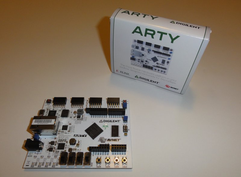
Arty is a Xilinx Artix FPGA evaluation kit from Digilent. At $99 you will get an Artix XC7A35T FPGA board + a Vivado design suite license. So basically everything that is needed to start experimenting with programmable logic design. 🙂

arty-01

Here are the detailed board contents:

  • Xilinx Artix-7 XC7A35T-L1CSG324I FPGA
  • On-chip analog-to-digital converter (XADC)
  • Programmable over JTAG and Quad-SPI Flash
  • 256 MB DDR3L with a 16-bit bus @ 667 MHz
  • 16 MB Quad-SPI Flash
  • 10/100 Mb/s Ethernet
  • USB-UART Bridge
  • Switches, Buttons, RGB LEDs
  • Four Pmod interfaces (32 I/O)
  • Arduino/ChipKit “shield” connector (49 I/O)

And the block diagram.

Arty-Kit-01

The Artix FPGA (Field Programmable Gate Array) device contains a large number of configurable logic blocks (CLBs), memory blocks, DSP blocks (multiplier/adder combination) and some other special purpose blocks (like A/D converters). All these blocks can be configured to form the desired logic functionality. The configuration is stored into SRAM type internal latches. The configuration storage is volatile and thus must be reloaded whenever the device is powered up. However, it is also possible to store the configuration into an external flash memory for automatic loading at power-up.

The part name gives us some basic information about the FPGA, e.g. the rough size as the number of available logic cells (35K), the speed grade (-1L = low power), the package pin count (324) and the temperature range. The speed grade basically defines the maximum clock speeds that can be obtained. The RoHS classification (6/6 w/ exemption 15) indicates that the package is almost lead free (lead only in solder).

device-code

More details of the device are shown in the table below.

6-input LUTs (look-up tables) 20800
Logic Cells (= 1.6 x number of LUTs) 33280
Slices ( = 3600 SLICEL + 1600 SLICEM = number of LUTs/4) 5200
CLB Flip-Flops (= 2 x number of LUTs) 41600
Block RAM/FIFO w/ ECC (36 Kb each) 50
Total Block RAM (Kb) 1800
CMTs (Clock Management Tiles containing 1 MMCM + 1 PLL) 5
Maximum Single-Ended I/O 210
Maximum Differential I/O Pairs 101
DSP Slices 90
Analog Mixed Signal (AMS) / XADC (dual 12-bit 1Msps ADC) 1
Configuration AES / HMAC Blocks 1

One logic cell corresponds to one 4-input LUT plus one flip-flop (this was the basic building block in the older FPGA devices). Now that there are 6 inputs in one LUT and 2 flip-flops the number of logic cells is approximated by the factor of 1.6.

From the 324 device pins 210 are available for user I/O.  The rest are reserved e.g. for device configuration, clock input, VDD and GND.

User I/O pins (I/O voltage from 1.2V to 3.3V) 210
Configuration and other special purpose pins 21
VDD and GND pins 93
Total number of pins 324

In the Arty board 129 of the 210 user I/O pins are reserved for connecting the switches and LEDs, the ethernet port, the SDRAM and the FLASH memory. From the rest of the user I/O pins 32 pins are available via the 4 PMOD (Peripheral Module) headers and 49 pins via the Arduino/chipKIT Shield Connector.

Artix FPGA architecture

The Artix XC7A35T FPGA device layout is illustrated in the figure below. The device is constructed from a set of logic blocks. At the edges there are the I/O blocks, then the clock management tiles (CMT) and in the center 6 logic tiles consisting of configurable logic blocks (CLB), block RAMs (BRAM) and DSP slices (DSP). There are also some special blocks (XADC, PCIe, GTP). The high speed serial interfaces in the GTP block are not bonded out to the FPGA package pins so they cannot be used in this device. Actually the device is identical to the larger XC7A50T device except that some of the blocks are disabled.

One logic tile, one CMT and one I/O bank form a clock region. Each clock region can have its own clock source. The clock source may be an external clock (each I/O bank contains clock capable input pins) or an internal clock generated with one of the CMT tiles (external reference clock is still needed). Each CMT-tile contains one MMCM (Mixed-Mode Clock Manager) and one PLL (Phase-Locked Loop). All in all there are 32 global clock lines in the FPGA. The clock lines are routed via the clocking backbone and in the HROW lines in the center of each clock region (one region can have up to 12 clocks).

In the Arty board there is a 100 MHz clock oscillator that is driving an MRCC (Multi-Region Clock Capable) pin E3 in the I/O bank 35.

Artix35T-Layout-02

Every CLB contains two slices and each slice contains 4 LUTs and 8 Flip-Flops. There are two kinds of slices, SLICEL and SLICEM. The SLICEM type can also be configured as a memory block with 256 bits or a 128-bit shift register. One CLB may contain either two SLICELs or one SLICEL and one SLICEM.

Each block RAM block contains a 36Kb memory array.  The array can be accessed with different configurations ranging from 32k x 1 bit to 512 x 72 bits. Both single and dual-port modes are supported. Several block RAMs can be combined to form a bigger RAM.

Arty-BlockRAM

One DSP slice contains a 25 x 18 bit multiplier and a 48-bit accumulator.  There is also a 25-bit pre-adder and a pattern detector and other functionality that e.g. allows cascading the slices to form different kinds of digital filter structures. The accumulator unit can also perform logical operations and it can be used as an up-down counter.

Arty-DspSlice-01

References

More details of the CLBs, Block RAMs and DSP Slices are available in the Xilinx web site.

UG474 – 7 Series FPGAs Configurable Logic Block User Guide

UG473 – 7 Series FPGAs Memory Resources User Guide

UG479 – 7 Series FPGAs DSP48E1 Slice User Guide