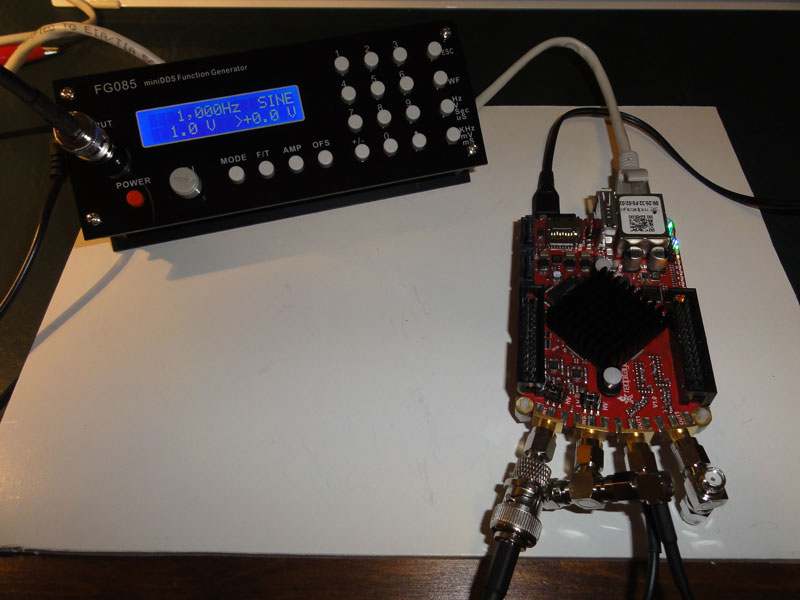
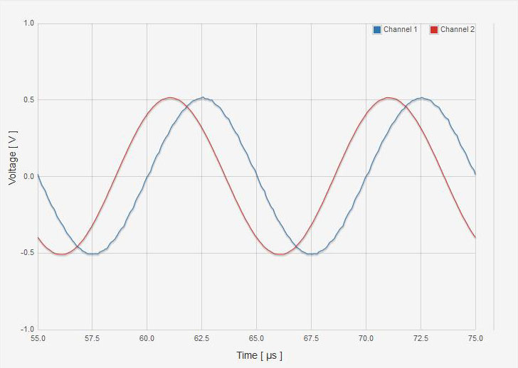
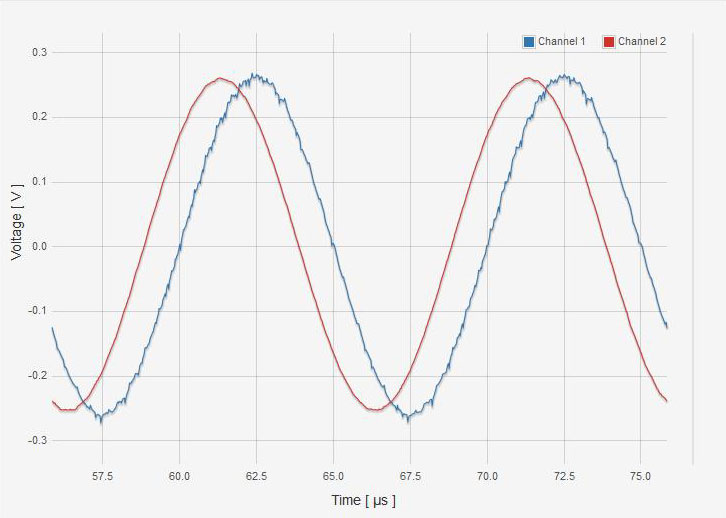
Ok, so now that I have assembled the FG085 board let’s see how the signals look like. Actually I could analyze the generated signal with my Red Pitaya. So let’s hook up the FG085 to Red Pitaya and power up both devices.
As the Red Pitaya also has a signal generator why not compare the two? Let’s start with the standard 1 kHz sine wave.
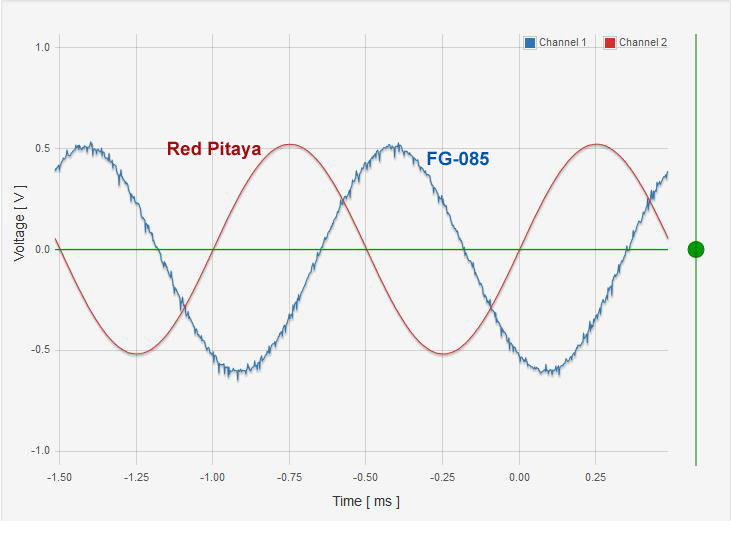
Hmm, the FG085 output looks a bit noisy. And there is some DC offset, too.
Then let’s try a triangle wave and let’s set the frequency to 100 kHz.
Not very clean either compared to Red Pitaya.
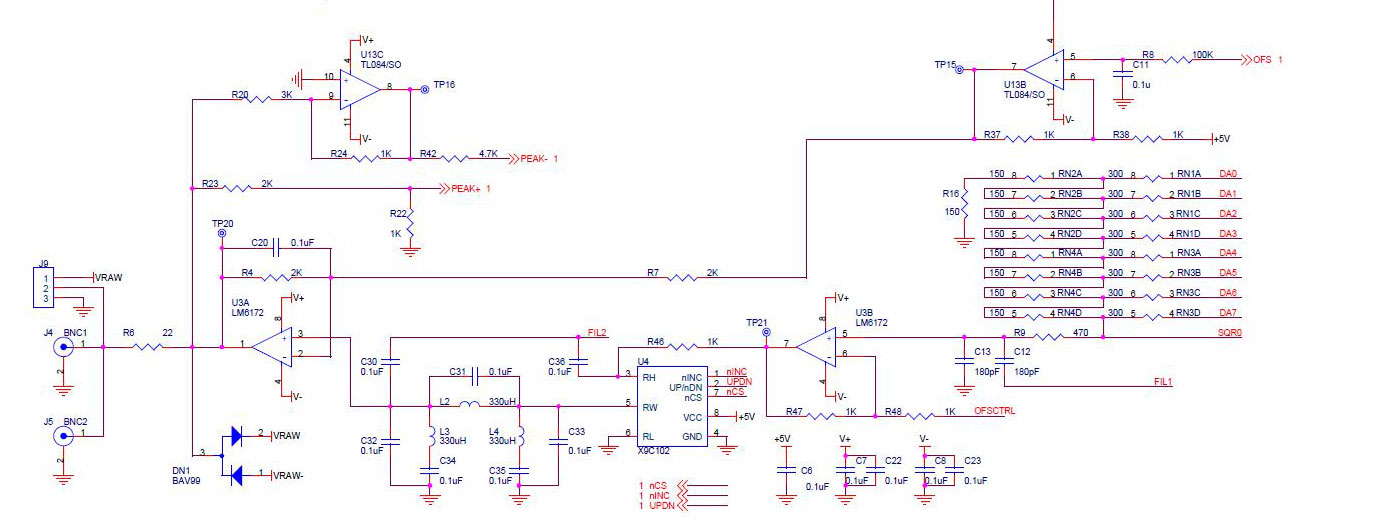
Looking at the FG085 schematics it looks like the signal is generated by an ATMega48 (running at 20 MHz). Eight digital output pins (DA0-DA7) are connected to an R-2R ladder D/A converter.
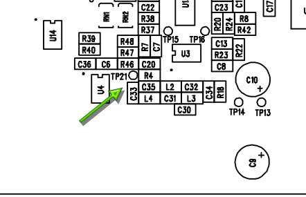
The output from the resistor network is connected to an opamp and there seems to be a test point at the opamp output (TP21). The test point can be located from the board assembly figure.
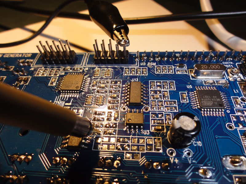
Let’s probe the test point.
The J8 header has two adjacent ground pins so that’s an easy place to hook up the negative probe cord. The output voltage seems to exceed Red Pitaya 5V range so let’s switch the probe to 10x.
Not so bad taking into account the 8-bit resolution. The frequency is still 100 kHz (T=10μs). The amplitude is 10 Vp-p which may make it harder to see the noise, though. Next in the signal path there is a digitally controlled potentiometer X9C102. Let’s probe the output pin RW (U4 pin #5 i.e the bottom pin on the right hand side).
Ok, so the noise becomes visible here. Where does it come from? Maybe we have some kind of a ground noise problem here. It could be that the analog and digital grounds are not properly isolated. The digital logic may draw quite big currents from the power supply when the logic switches state at every clock cycle (20 MHz in this case). If the large current spikes are allowed to travel through the analog ground wires we will have fluctuations (=noise) in the analog signals. The noise amplitude would vary depending on the number of logic elements switching at the same time.
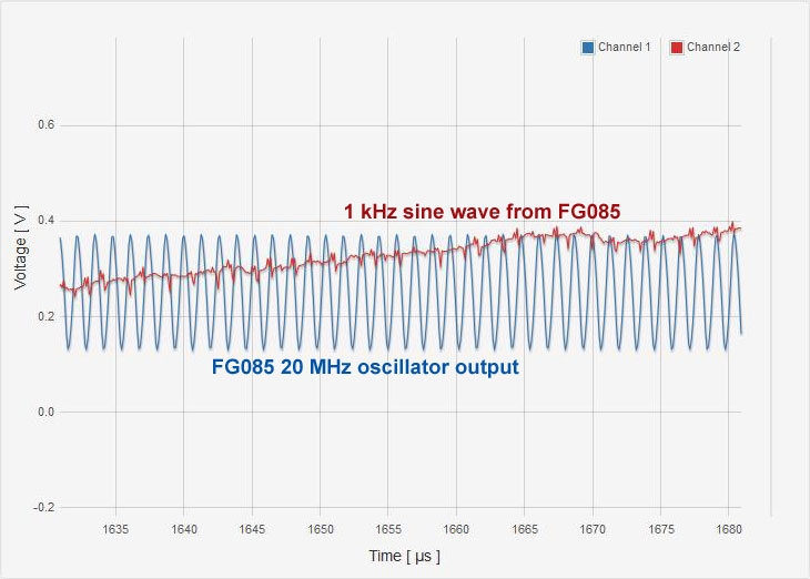
Let’s capture the 1 kHz sine wave again and let’s connect another probe to the FG085 oscillator test point TP22.
I would say the noise spikes match quite well with the clock transitions.
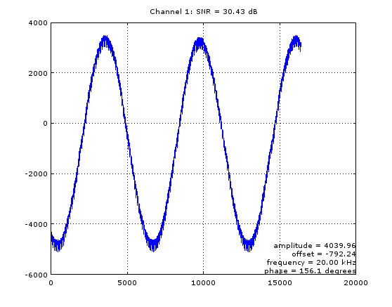
We can also get some quantitative figures by acquiring the samples from Red Pitaya and analyzing them in Octave. E.g. we could calculate the signal-to-noise ratio and compare the two generators.
Below is the captured signal from FG085. SNR is 30.43 dB.
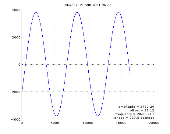
We can compare this to signal generated by Red Pitaya. The SNR is 52 dB so there is about 20 dB improvement.
What if one of the bigger capacitors was badly soldered? These bypass capacitors are there to reduce the voltage fluctuations in the power supply lines. Unfortunately the LCD display now blocks access to those capacitors and I think it is impossible to remove the display anymore (too many pins soldered). So it looks like there is very little I can do the improve that situation.
Oh well, maybe I’ll stick to my Red Pitaya. 🙂
