The next step I’m going to try with the Arty board is to connect the 100 MHz clock signal to the FPGA. That will enable me to start experimenting with sequential logic design.
As mentioned at the end of the previous post Digilent provides a master constraint file (Arty_Master.xdc) that defines all the FPGA pin connections for us. For the clock signal the file also specifies the clock period (10ns) and duty cycle (50%). The clock port name is CLK100MHZ but let’s change that to ‘clk’ for simplicity.
## Clock signal

set_property -dict {PACKAGE_PIN E3 IOSTANDARD LVCMOS33} [get_ports {clk}]
create_clock -period 10.0 -name sys_clk_pin -waveform {0.0 5.0} -add [get_ports clk]
Let’s create a simple binary counter and display the counter 4 MSBs with the 4 blue leds. If we step the counter directly with the provided clock the LSB will cycle at half the clock rate, i.e. at 50 MHz. And generally any bit N will cycle at 50/2^N MHz. For bit 25 would mean 1.49 Hz which is slow enough I think. So let’s design a 29-bit counter and connect bits 25 to 28 to the LED outputs.
I’ll add the blue led ports from the Arty_Master.xdc to my local constrain file.
set_property -dict {PACKAGE_PIN E1 IOSTANDARD LVCMOS33} [get_ports {led0_b}]
set_property -dict {PACKAGE_PIN G4 IOSTANDARD LVCMOS33} [get_ports {led1_b}]
set_property -dict {PACKAGE_PIN H4 IOSTANDARD LVCMOS33} [get_ports {led2_b}]
set_property -dict {PACKAGE_PIN K2 IOSTANDARD LVCMOS33} [get_ports {led3_b}]
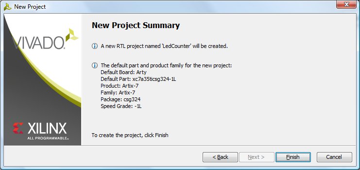
Let’s start Vivado and create a new project (RTL project like before) called LedCounter.
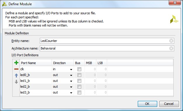
First I’ll create a new constraint file (LedCounter.xdc) and add the clk and led port definitions there. Then as before I’ll add one VHDL module called LedCounter which has one clock input port and 4 LED output ports.
Now we have the VHDL entity which defines the module port interface and an empty architecture part where we should describe the implementation.
For the counter we will need to add a clocked process. You don’t need to remember the exact VHDL syntax as you can go to Window>Language Templates>Synthesis Constructs>Process>Posedge Clocked>/w Sync Low Reset and copy the template code from the preview window into the architecture section. We don’t actually need the reset (as all the registers in the FPGA will be automatically reset during the configuration phase) so I’ll remove that part.
In addition we will need to define one signal that represents the counter value. That will go to the architecture declaration part located before the ‘begin’ statement.
Here is the complete design:
library IEEE;
use IEEE.STD_LOGIC_1164.ALL;
use IEEE.NUMERIC_STD.ALL;

entity LedCounter is
   Port ( clk : in STD_LOGIC;
          led0_b : out STD_LOGIC;
          led1_b : out STD_LOGIC;
          led2_b : out STD_LOGIC;
          led3_b : out STD_LOGIC);
end LedCounter;

architecture Behavioral of LedCounter is
   signal counter : UNSIGNED(28 DOWNTO 0);
begin
process (clk)
begin
   -- count from 0 to 2^29-1 and wrap around
   if (clk'event and clk = '1') then
      counter <= counter + 1;
   end if;
end process;
-- connect the 4 MSBs to the blue LEDs
led3_b <= counter(28);
led2_b <= counter(27);
led1_b <= counter(26);
led0_b <= counter(25);
end Behavioral;
The counter signal type is UNSIGNED. This type is defined in the IEEE.NUMERIC_STD package so we will need to uncomment that line from the template. The counting is done inside the clocked process, counter will be incremented by one every clock cycle (at 100 MHz). At the end we have the four LED ports connected to the 4 MSBs of the counter.
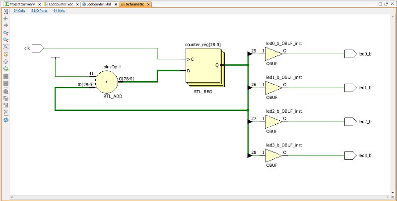
Let’s go to the Flow Navigator and select RTL Analysis > Elaborated Design > Schematic. This will make Vivado to check the VHDL design and display the high-level design schematic. Looks ok to me.
So now we can go and click “Generate Bitstream”. Vivado will first synthesize and implement the design and then create the configuration bit file. Looking at the project summary page there is one Design Rule Check warning:
[DRC 23-20] Rule violation (CFGBVS-1) Missing CFGBVS and CONFIG_VOLTAGE
Design Properties - Neither the CFGBVS nor CONFIG_VOLTAGE voltage property
is set in the current_design.
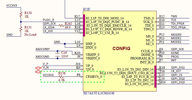
This does not seem to cause any issues but let’s see if we can correct that anyway. Looking at the Arty schematics we can see that the CFGBVS input pin is driven by a 3.3V voltage source.
The warning message has some instructions how to correct the issue, basically we should just add two properties to our constraint file. That’s easy to fix:
set_property CONFIG_VOLTAGE 3.3 [current_design]
set_property CFGBVS VCCO [current_design]
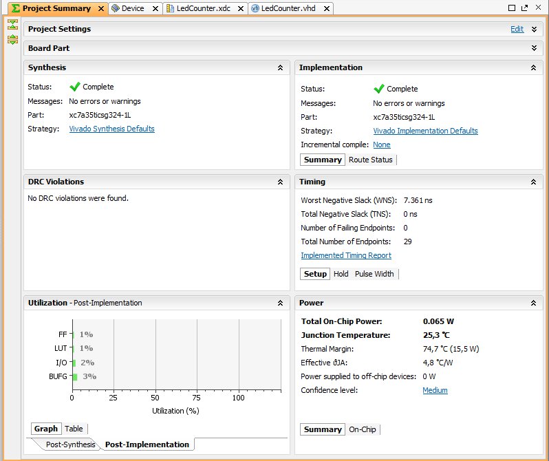
After a second synthesis/implementation round the project summary looks like this. Seems the logic utilization figure is quite negligible compared to the available resources.
Onwards. Let’s connect Arty and program the FPGA: Open Target and Program Device. Blue LED’s start counting immediately. Nice.
Hi EB! I just bought an Arty a week ago and have followed through all your posts so far to set up Vivado and get my Arty up and running. Really enjoyed the simple tutorials, they are super helpful, easy to follow and have shown me where to look for the information I need for some bigger projects (the Arty Master xdc was a godsend). I hope you’re doing some more!