At the heart of the Arduino Uno there is the ATMEL ATmega328 microcontroller. Maybe I should take a quick look at the device and its capabilities before diving into more programming.
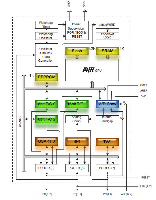
Below is the ATmega328 block diagram. The memory subsystem consists of:
- 32 KB Flash memory (used as program memory)
- 2 KB SRAM (used as data/stack storage)
- 1 KB EEPROM (for any other persistent storage needs)
Looks like the CPU is based on Harvard architecture as the program and data memories are separated.
There are 3 timer/counter blocks and 1 A/D converter with 10 bit resolution (6 analog inputs can be multiplexed to the converter input). In addition there is a temperature sensor than can also be connected to the ADC.
For communication there are
- USART (Universal Synchronous/Asynchronous Receiver/Transmitter)
- SPI (Serial Peripheral Interface)
- TWI (Two Wire Interface a.k.a I2C)
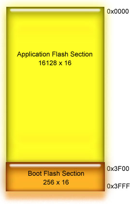
The program memory map consists of 16K x 16 bit words. The last 256 words (0.5 KB) are reserved for the bootloader code.
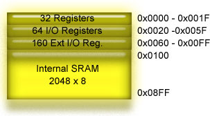
The data memory consists of 4 parts:
- 32 CPU registers are mapped to the first 32 bytes.
- 64 I/O registers.
- 160 Extra I/O registers.
- Internal 2KB SRAM.


